
 Computer Forum
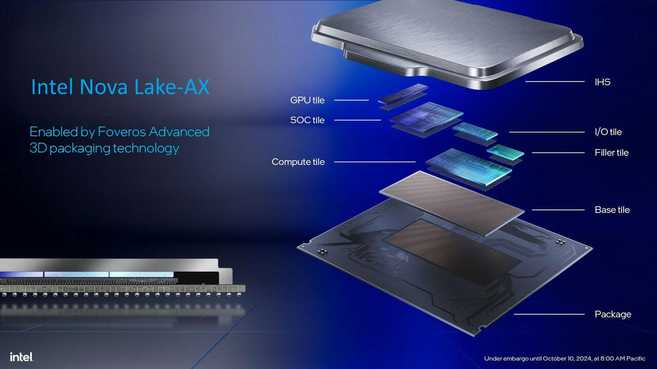 Intel Nova Lake AX Details (Image © Intel)
Core Ultra 9 4995HX
The Core Ultra 9 4995HX is designed for ultra-enthusiast laptops and mobile workstations. This processor features a total of 28 cores and 28 threads and utilizes a hybrid architecture spread across three different core types:
- P-cores: 8 performance cores based on the Coyote Cove architecture.
- E-cores: 16 efficiency cores based on the Arctic Wolf architecture.
- LP-E-Cores: 4 low-power efficiency cores, also based on the Arctic Wolf architecture.
The 4995HX uses a single-compute-module configuration, which corresponds to the design of the single-module desktop variants. While desktop versions of Nova Lake can reach up to 52 cores across two compute modules, the mobile HX series is limited to a single-module layout. This specific chip supports a large cache capacity of up to 144 MB BFC (bLLC). The graphics component consists of two Xe3 iGPU cores.
Core Ultra 9 4970H
The Core Ultra 9 4970H is designed for high-performance thin-and-light or gaming laptops. It features a 16-core configuration consisting of 4 P-cores, 8 E-cores, and 4 LP-E-cores. The number of cores remains unchanged from earlier Panther Lake-H designs. The 4970H offers a significant improvement in integrated graphics. It is equipped with up to 12 Xe3P iGPU cores, which is expected to result in a substantial increase in graphics performance compared to previous generations.
There are significant differences in power consumption between the HX and H series. The Nova Lake-HX models are designed for maximum throughput and high thermal limits, while the H series is optimized for a balance between performance and efficiency.
- Nova Lake-HX: Rated power is estimated to range from 55 W to a maximum of 160 W.
- Nova Lake-H: Rated power is estimated to range from 28 W to approximately 115 W.
Manufacturing Process and Chip Dimensions
The Nova Lake-HX processors are manufactured using TSMC’s N2P process. Although the first engineering samples (ES1) were produced using 18A-P technology, the external TSMC node is planned for the final commercial devices.
The final compute die for the N2P variant measures 14.8 mm × 6.6 mm, corresponding to a total chip area of 97.68 mm². This represents a reduction in size compared to the larger ES1 variant, bringing its width in line with that of the 4+8-core configurations.