
 Computer Forum
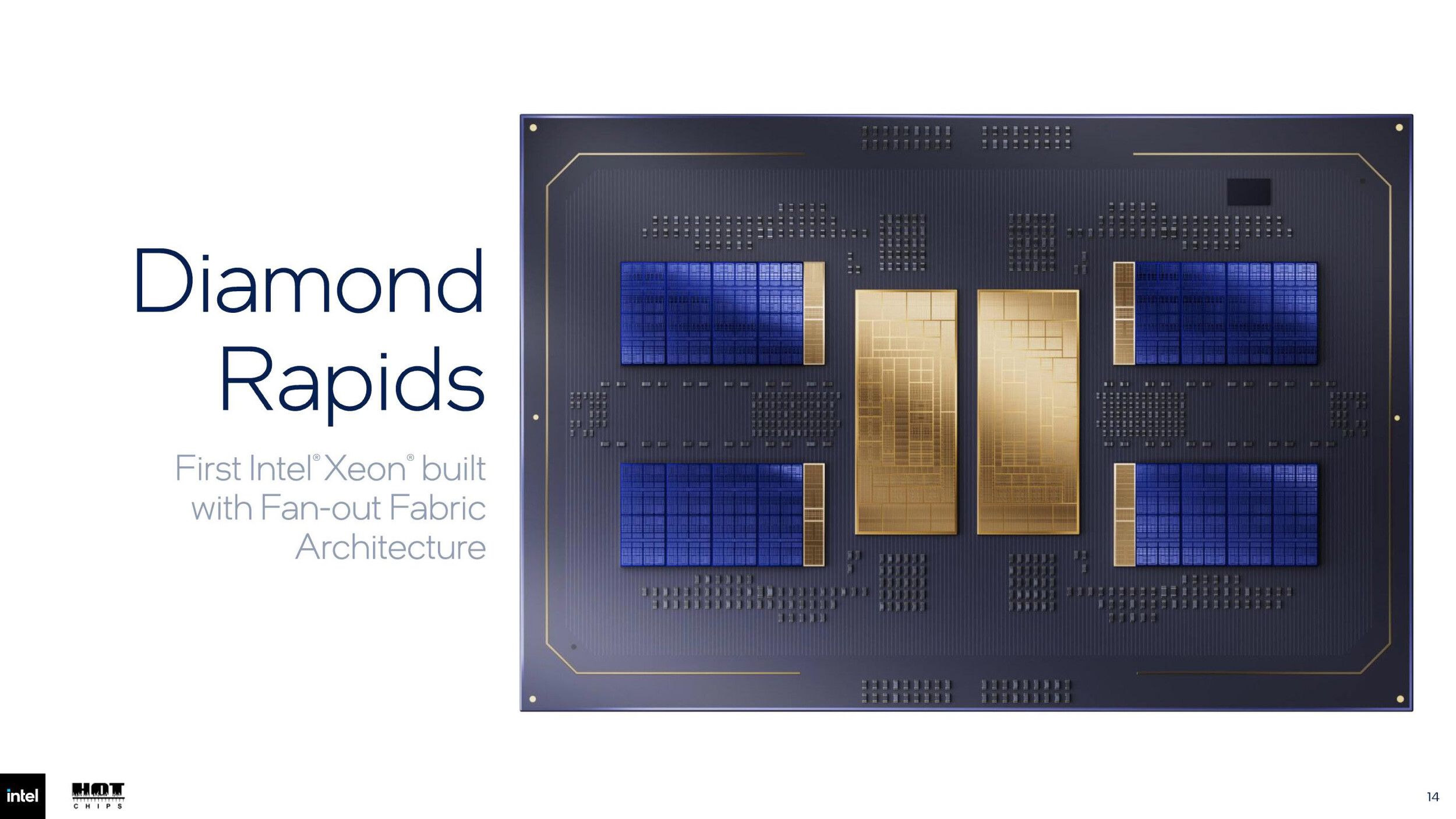 Intel Diamond Rapids Design (Image © Intel)
Intel has unveiled its new UCIe technology for both Diamond Rapids and Wildcat Lake. With this, the manufacturer aims to reduce production costs and improve chip yield. In the Diamond Rapids architecture, up to four stacks consisting of cache and processor cores are connected via this interface. Although both product families use UCIe, there is a difference in bandwidth: Diamond Rapids uses transceivers operating at 16 GT/s, while Wildcat Lake operates at 8 GT/s.
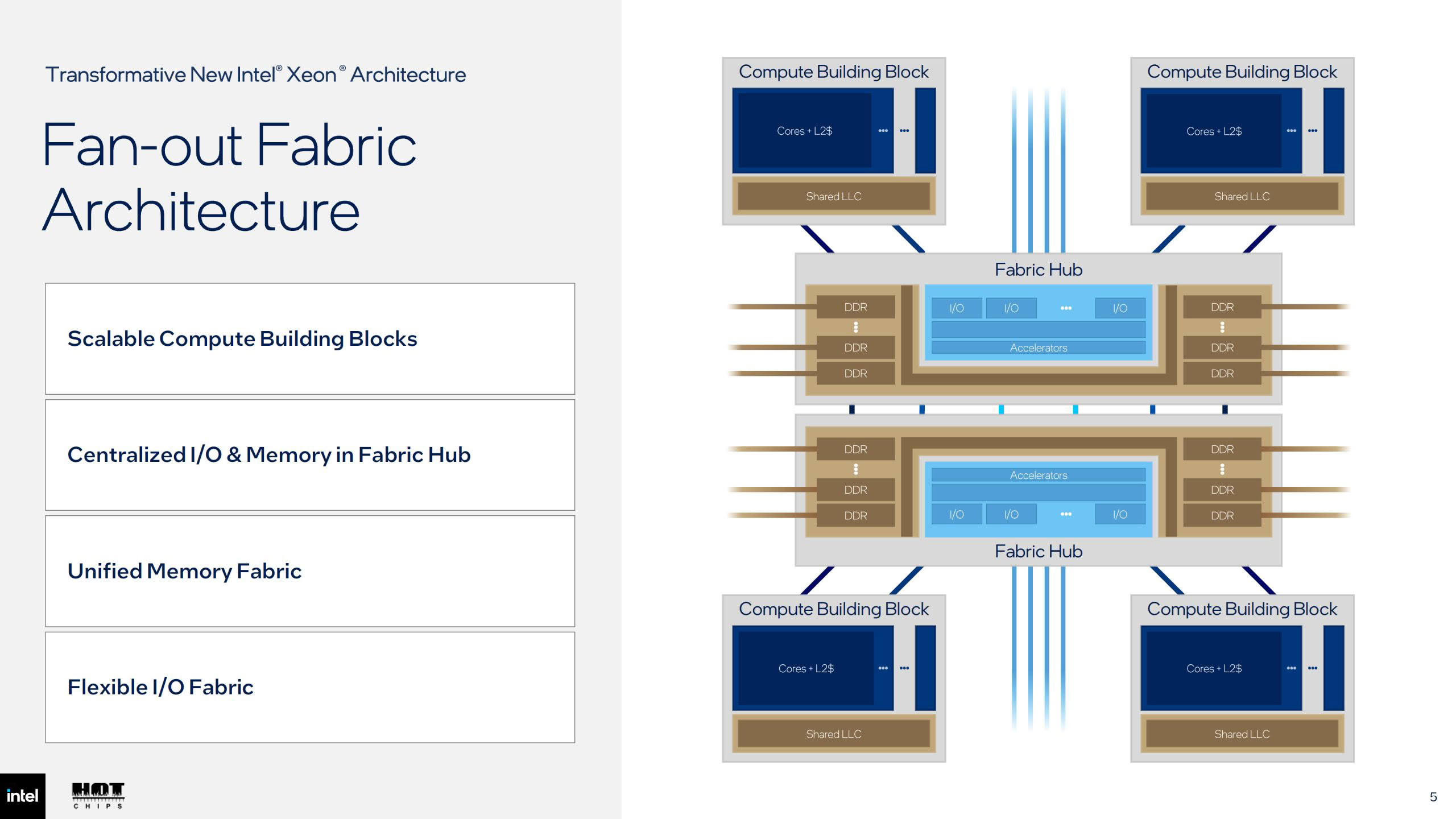 Intel Diamond Rapids Fabric (Image © Intel)
The system topology calls for two CBBs to be connected to a central “Fabric Hub Tile.” This hub integrates the following components:
- Eight memory controllers with support for Compute Express Link (CXL) and data encryption.
- 64 transceivers for PCIe 6.
- Plus additional PCIe Gen 4 lanes
- L3 shared cache as the lower tile
- Compute tiles connected to a fabric hub. The two hubs have a faster connection.
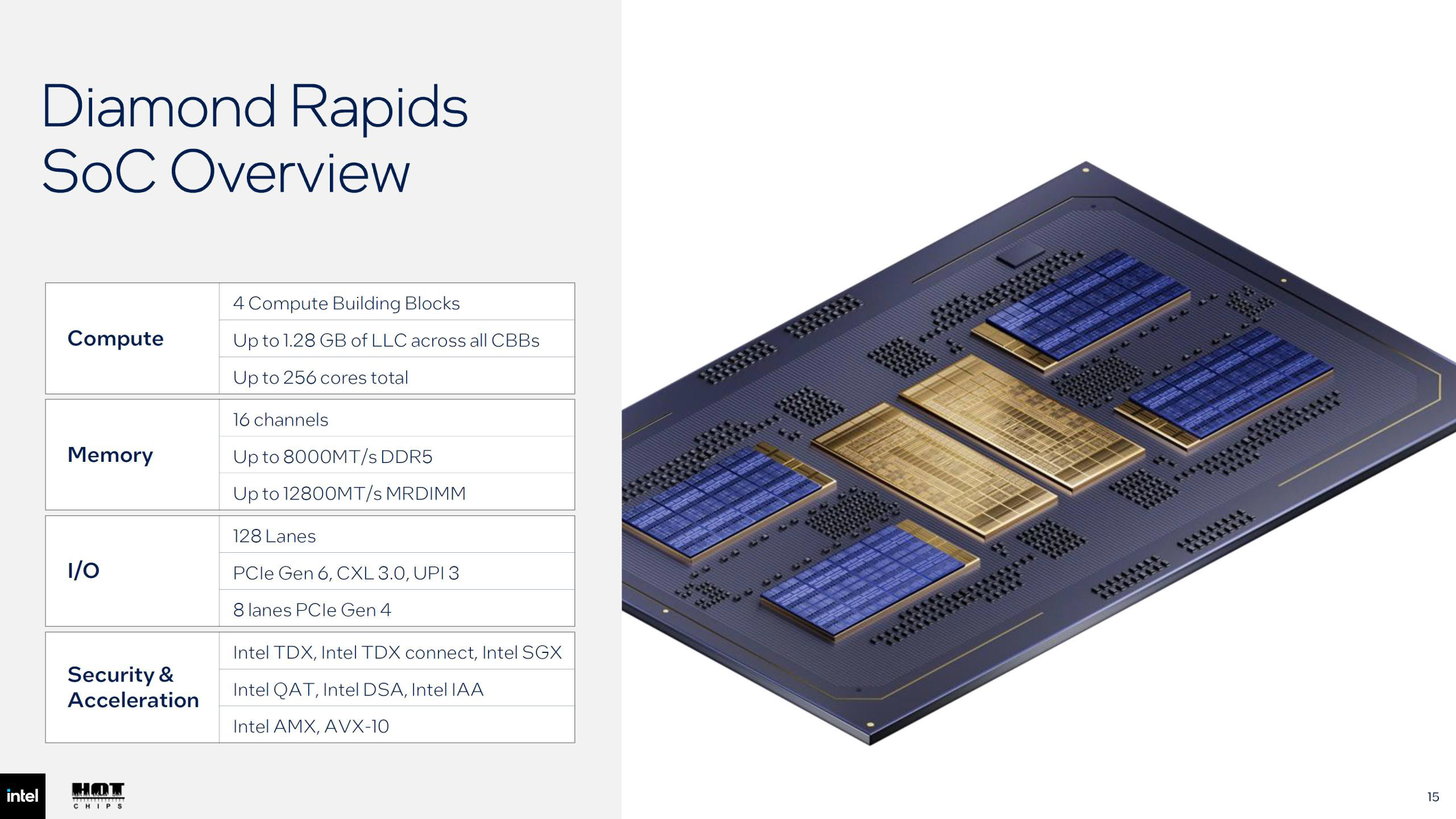 Intel Diamond Rapids SoC (Image © Intel)
Memory Bandwidth and Memory Specifications
Diamond Rapids supports high-speed memory configurations for intensive server workloads. With standard DDR5 DIMMs, the system achieves speeds of 8,000 MT/s. For higher performance requirements, multi-rank DIMMs ([MRDIMMs][1]) enable speeds of up to 12,800 MT/s, resulting in a total memory bandwidth of 1.6 TB/s—or 400 GB/s per core tile.
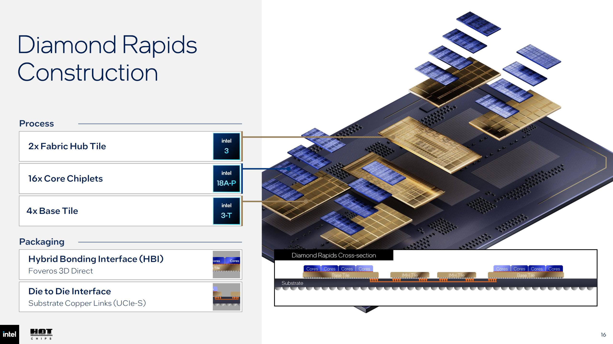 Intel Diamond Rapids Architecture (Image © Intel)
Chiplet Design and Manufacturing Process
Intel has adjusted the relationship between the last-level cache (LLC) and the memory controller, splitting them into separate units. The core chiplets are positioned on an active base tile, similar to the Clearwater Forest design. This configuration enables a distributed L3 cache that can potentially reach 1.28 GB of LLC and uses a distributed snoop agent to minimize communication latency within the processor.
Manufacturing takes place using two processes:
- Core chiplets: Manufactured using the optimized Intel 18A-P process.
- Supporting chiplets: Manufactured using the Intel 3 (3 nm) process.
Each core chiplet contains 16 P-cores, enabling a maximum configuration of 256 cores per socket.
Instruction Set and Performance Enhancements
The upcoming processors will introduce Advanced Performance Extensions (APX). This update doubles the number of general-purpose registers and introduces new conditional instructions that allow the processor to execute instructions based on specific conditions, potentially increasing execution speed. Additionally, the architecture supports AVX 10.2 and Advanced Matrix Extensions (AMX) for accelerated mathematical calculations. [1]: https://www.pcmasters.de/server/133716142-ddr5-mrdimms-verlaengern-die-lebensdauer-von-servern-durch-anpassung-an-die-ddr6-bandbreite.html