
 Computer Forum
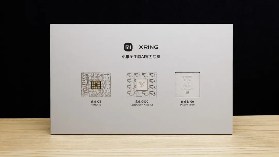 Xiaomi XRing Versionen (Image © weixin)
XRing O3: Technical Specifications of the Flagship AI SoC
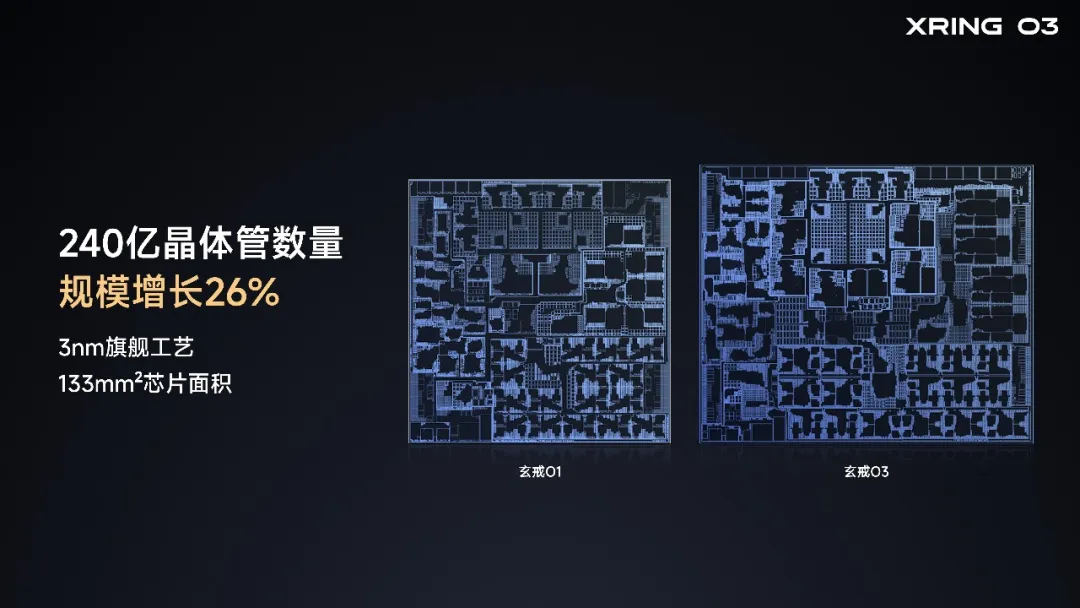
The XRing O3 is manufactured using a 3-nm process and features 24 billion transistors on a chip area of 133 mm². To increase transistor density by 5%, Xiaomi has implemented “Top Channelless” technology, which eliminates conventional power supply channels, allowing components to be packed more tightly. The chip also utilizes an expanded library of over 2,400 standard cells for improved efficiency.
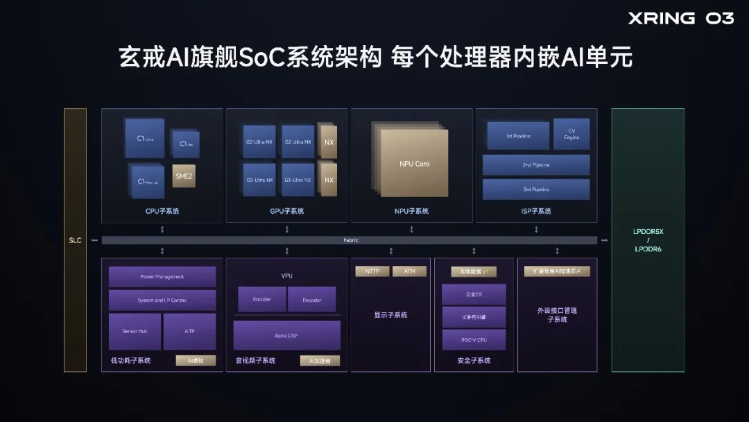 Xiaomi XRing O3 Architektur (Image © weixin)
CPU and GPU Performance
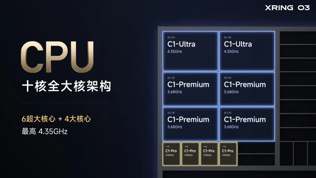
The processor features an “All-Big-Core” architecture consisting of ten cores: six “Super-Big-Cores” and four “Big-Cores,” with maximum clock speeds of up to 4.35 GHz. In benchmark tests, the SoC achieved single-core scores of 3,945 and multi-core scores of over 15,000 in Geekbench 6.5. Power consumption during everyday workloads has been reduced by 25% compared to the previous O1 generation.
 Xiaomi XRing O3 Aufbau (Image © weixin)
The graphics section features a 16-core G2 Ultra NX GPU with support for advanced ray tracing. Performance metrics show significant increases:
- GFXBench Aztec Ruins (1440p): 94% increase.
- 3DMark Steel Nomad Light: 85% increase.
- 3DMark SolarBay Extreme (Ray Tracing): 182% increase.
- **Despite these increases, the GPU’s power consumption has dropped by 64%. Memory and Latency Optimization
 Xiaomi XRing 03 Chip (Image © weixin)
The Xring O3 is the first mobile SoC to support LPDDR6 memory, which increases the single-channel width from 16 bits to 24 bits and boosts bandwidth to 113.8 GB/s. To minimize data access latency to 82 ns, Xiaomi has implemented three specific optimizations:
- 1. Unified Fusion Bus: A unified protocol for the entire memory path, reducing conversion overhead by 75%.
- 2. Physical Routing: Special high-alloy metal layers between the SLC and the memory controller to reduce impedance.
- 3. Data Prefetching: A system that initiates memory requests while simultaneously searching lower-level caches.
The chip includes 12 MB of L2 cache, 16 MB of L3 cache, and a 16 MB System Level Cache (SLC).
 Xiaomi XRing 03 (Image © weixin)
AI Integration and NPU Architecture
The NPU, developed for large language models (LLMs), delivers 200 TOPS of Tensor computing power (A8W4) and features a vector unit with 3.13 TFLOPS. Xiaomi has introduced the MiMo 5 quantization model, which uses a five-value system in combination with lossless Huffman hardware compression to reduce memory bandwidth requirements by 30% without compromising inference quality.
AI acceleration is integrated into all modules:
- CPU: Two matrix computing units with SME2 technology (3.5 TOPS).
- GPU: Eight NX neural accelerators (36 TOPS) for AI super-resolution and image interpolation.
- ISP/DPU/ADSP: Integrated hardware for noise reduction in night shots, intelligent resolution optimization, and audio echo cancellation.
 Xiaomi XRing O100 (Image © weixin)
XRing O100: High-Bandwidth AI Accelerator
The XRing O100 is a dedicated AI acceleration chip that utilizes 6-nm 3D wafer-level stacking technology. It overcomes the memory barrier through the use of wafer-on-wafer packaging, where data paths are shifted from planar routing to vertical interconnects to enable memory-proximate data processing.
Key technical features include:
- Hybrid bonding: A bond pitch of 1.4 μm, which eliminates the need for conventional micro-bumps and thus increases connection density.
- Face-to-Face (F2F) structure: Direct metal-to-metal connections between DRAM and NPU layers to minimize physical distance.
- Bandwidth: Achieves a total bandwidth of 1.22 TB/s, which is approximately 16 times faster than LPDDR5X memory.
- Matrix bus: A high-bandwidth bus that dynamically switches between ring topology (for prefill) and broadcast topology (for decode).
 Xiaomi XRing D100 (Image © weixin)
Xring D100: Processor for Autonomous Driving
The Xring D100 is a high-performance 3-nm chip designed specifically for autonomous driving. It features a 20-core CPU and a 16-core NPU and supports up to 160 GB of unified memory. The architecture enables the local deployment of large models with up to 200 billion parameters. The D100 is expected to enter commercial use next year.