
 Computer Forum
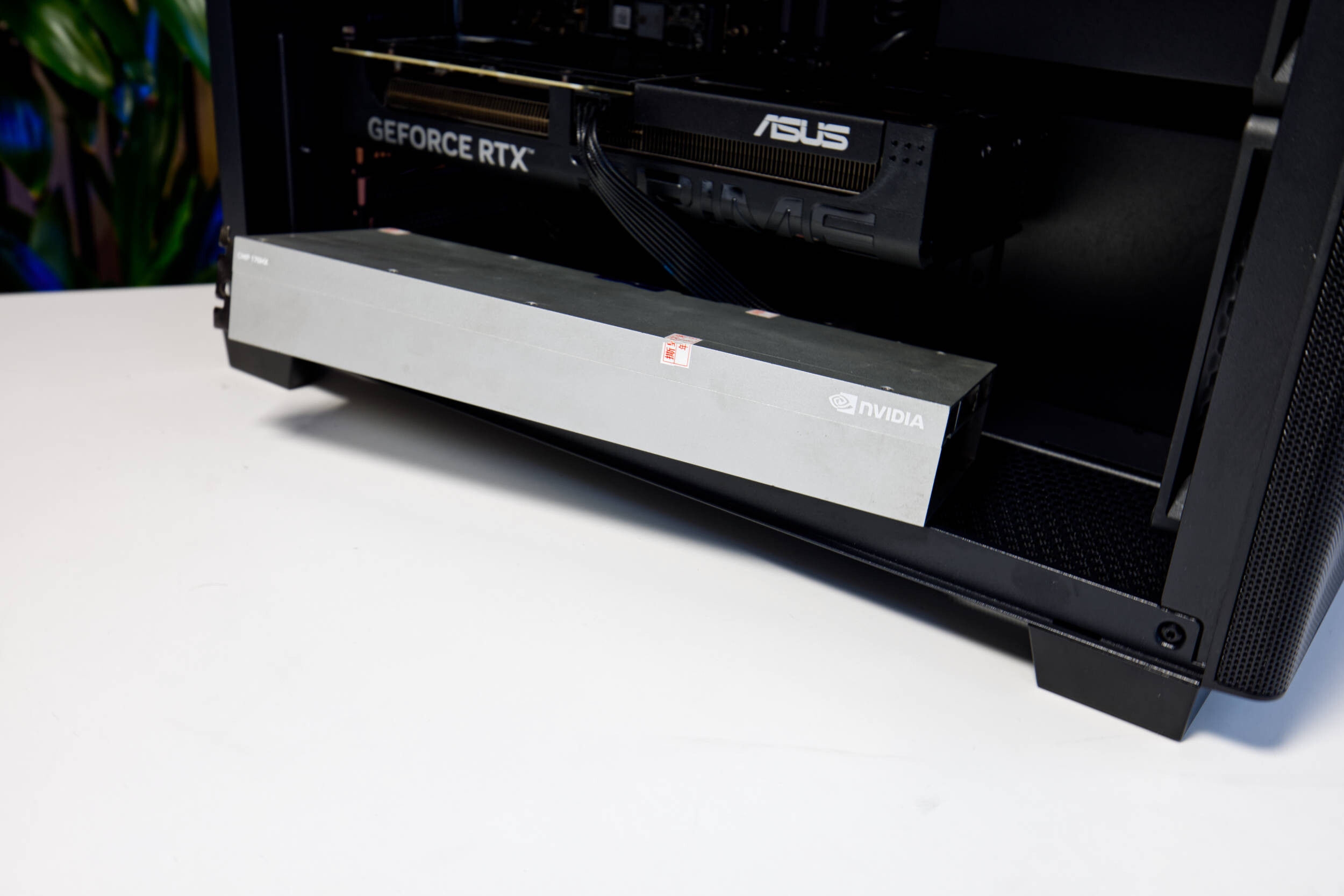 NVIDIA CMP 170HX Unlock (Image © PCMasters.de)
Voltage Fault Injection and Fuse Programming
This new modification differs from the previous software-based unlock method, cmpunlocker, which we reported on and also used with our card. So far, we’ve managed to unlock the memory from 8 GB to 64 GB and thereby gained access to some key features like ECC. Now, however, we need to take it a step further and use a microcontroller to generate voltage faults during the GPU’s boot sequence.
By manipulating the voltage at precise intervals, the researcher was able to bypass the limitations associated with the GPU’s fuse programming. This enables a permanent reconfiguration of the GPU, allowing it to recognize and utilize memory partitions and computing units that were disabled at the factory. The memory is present from the factory because NVIDIA cannot remove the defective HBM memory during manufacturing. It is therefore present but otherwise locked down.
Memory Capacity and Computing Units
Test results show a high success rate for memory unlocking. Of ten 8-GB CMP-170HX units tested, nine were successfully unlocked to their full capacity of 80 GB, although one card remained limited to 64 GB. NVIDIA sold the cards as “downgraded”—those with defects or that did not meet NVIDIA’s specifications—so the silicon may also be defective. For the 10-GB version of the card, the modification resulted in a usable storage capacity between 40 GB and 48 GB.
The researcher also expanded the GPU’s computational resources. The number of active streaming multiprocessors (SMs) increased from the factory default of 70 to between 120 and 126 units.
What were the results?
The increase in computing units leads to a measurable performance boost in floating-point operations. In OpenCL FP16 FMA benchmarks, the modified CMP 170HX achieved 85.86 TFLOPS. This figure surpasses the 72.49 TFLOPS measured for a standard off-the-shelf NVIDIA A100 accelerator.
To further align the card’s functionality with professional accelerators, additional modifications were made at the board level to enable the following:
- PCIe Gen 4 support for higher data transfer rates.
- NVLink connectivity for multi-GPU scaling.
Above all, NVLink is a major bonus, as the severely limited bandwidth between cards becomes a bottleneck when using multiple such cards. Until now, it was assumed that NVLink had been disabled due to missing components. The technical documentation, including firmware and hardware designs, has been made available via GitHub; however, the process requires physical modifications to the hardware and repeated voltage spikes. The documentation is also highly technical.